
Abstract
As switching frequencies climb into the hundreds of megahertz and PCB trace densities continue to increase, electromagnetic interference has become one of the most persistent obstacles between a working prototype and a certified product. System-level shielding and cable filtering address part of the problem, but high-frequency noise generated on the board itself demands a targeted, board-level response.
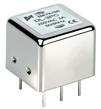
A PCB filter—whether implemented as a discrete LC network, a common-mode choke array, or an integrated π-network component—provides precisely that response. Placed at the right node during schematic capture, it intercepts conducted and radiated interference before it propagates across the board, couples onto power rails, or escapes the enclosure. The result is measurable insertion loss at the frequencies that matter most for CISPR 32, FCC Part 15, and IEC 61000-4 compliance.
This article walks procurement engineers and system designers through the root causes of board-level EMI, the filtering topologies available, the standards that govern selection, and the commercial scenarios where a dedicated PCB EMI suppression component delivers the greatest return. Actionable specification guidance is included throughout.
1. Understanding EMI Noise and Why Board-Level Filtering Matters
1.1 Root Causes of High-Frequency Interference on PCBs
EMI on a PCB originates from two primary categories: conducted interference, which travels along power and signal traces, and radiated interference, which couples through the air from high-dV/dt switching nodes or clock harmonics.
The dominant sources in modern designs include:
- Switch-mode power supply (SMPS) switching transients — MOSFETs and diodes generate steep voltage edges with harmonic content extending well beyond 100 MHz.
- Clock harmonics — a 50 MHz processor clock produces significant energy at the 3rd, 5th, and 7th harmonics (150 MHz, 250 MHz, 350 MHz), each a potential emissions violation.
- Power-line coupling — impedance discontinuities on the DC bus allow switching noise to back-propagate into shared supply rails, corrupting sensitive analog or RF front-ends.
- Ground bounce — simultaneous switching of high-speed digital outputs creates transient ground potential differences that radiate from PCB edge structures.
Understanding which mechanism dominates in a specific design is the first step toward specifying the correct PCB EMI filter topology and placement location.
1.2 Limitations of System-Level vs. Board-Level EMC Approaches
Chassis-level shielding and external line filters are effective at blocking interference entering or leaving the enclosure, but they cannot suppress noise that originates and circulates within the PCB itself. A switching regulator that injects 150 mV of ripple onto a 3.3 V rail will degrade ADC performance and increase radiated emissions from internal traces regardless of how well the enclosure is sealed.
Board-level EMC filtering closes this gap. By placing a high-frequency interference filter directly at the noise source—on the output of a DC-DC converter, at the input of a sensitive analog stage, or across a high-speed data line—the designer intercepts interference before it has the opportunity to couple to adjacent traces, radiate from PCB structures, or reach I/O connectors. In dense, high-speed designs where trace lengths act as efficient antennas at GHz frequencies, this localized suppression is not optional—it is a fundamental part of the signal integrity and EMC architecture.
2. How a PCB Filter Works: Core Principles and Topologies
2.1 Filtering Mechanisms — LC, RC, and π-Network Topologies
PCB filters operate on impedance mismatch: a reactive network presents high impedance to interference frequencies while passing the desired signal or DC power with minimal attenuation. The three primary architectures each suit different noise environments:
- LC low-pass filter — series inductor plus shunt capacitor. Ideal for power rail filtering where the cutoff frequency is set below the switching harmonic. Achieves steep roll-off with low DC resistance.
- RC filter — series resistor plus shunt capacitor. Lower cost and smaller footprint; suitable for low-current signal lines where the resistive voltage drop is acceptable.
- π-network (CLC) — shunt capacitor, series inductor, shunt capacitor. Provides the highest insertion loss per stage and is preferred for aggressive SMPS noise suppression or RF interference rejection above 100 MHz.
- Common-mode filter/choke — wound on a high-permeability ferrite core; attenuates common-mode currents flowing in the same direction on differential pairs without affecting the differential signal. Essential for USB, CAN, and Ethernet interfaces.
Insertion loss is the key performance metric, expressed in dB as the ratio of signal power delivered to a load without versus with the filter. A well-designed π-network PCB EMI suppression component can achieve 40–60 dB insertion loss at 100 MHz.
2.2 Component Selection and PCB Layout Considerations
Specifying the correct component is only half the task—layout determines whether the specified performance is realized in practice.
Critical layout rules include:
- Minimize loop area between the filter and the noise source to reduce parasitic inductance that degrades high-frequency performance.
- Maintain ground-plane continuity directly beneath filter capacitors; a split or interrupted ground plane increases return-path inductance and reduces effectiveness.
- Route filtered and unfiltered traces on separate layers to prevent capacitive coupling that bypasses the filter.
- Place filter components as close as possible to the noise source (SMPS output node, connector pin, or clock driver) rather than at the load.
Capacitor self-resonant frequency (SRF) must exceed the target suppression frequency; X7R and C0G ceramics in 0402 or 0201 packages offer SRF values above 500 MHz and are the standard choice for high-frequency PCB EMI filters.
| Filter Topology | Frequency Range | Insertion Loss | Impedance | Typical Application | Package |
|---|---|---|---|---|---|
| LC Low-Pass | 1–100 MHz | 20–40 dB | 50 Ω | DC-DC converter output | 0402 / 0603 |
| π-Network (CLC) | 10–500 MHz | 40–60 dB | 50 Ω | SMPS, RF power supply | Integrated module |
| RC Signal Filter | 1–50 MHz | 10–25 dB | High-Z | ADC input, sensor line | 0402 / 0201 |
| Common-Mode Choke | 1–1000 MHz | 30–50 dB | Differential | USB, CAN, Ethernet | SMD array |
| Band-Stop (Notch) | Narrow band | 20–40 dB | 50 Ω | Clock harmonic suppression | 0402 |
3. EMC Compliance Standards and Certification Requirements
3.1 Key International Standards Governing PCB-Level EMI Filters
Selecting a board-level EMC filter without reference to the applicable standard risks over- or under-specifying the component. The most commercially relevant standards are:
- CISPR 32 / EN 55032 — sets radiated and conducted emission limits for multimedia equipment across 30 MHz–1 GHz. Class B limits (residential use) are 10 dB more stringent than Class A, directly influencing required insertion loss values.
- FCC Part 15 Subpart B — U.S. equivalent for unintentional radiators; conducted limits apply from 450 kHz to 30 MHz, making low-frequency LC filter performance critical for power-line compliance.
- IEC 61000-4-4 / 4-6 — immunity standards covering electrical fast transients (EFT) and conducted RF immunity. PCB filters on I/O and power ports directly improve pass rates.
- IEC 61000-4-2 — ESD immunity; transient suppression filters at connector entry points reduce susceptibility to 8 kV contact discharge events.
Frequency band alignment between the standard’s test range and the filter’s specified insertion loss curve is the core matching exercise during component selection.
3.2 Qualification Testing and Documentation for Procurement
For regulated markets, component documentation is as important as electrical performance. Procurement teams should require:
- Insertion loss test reports measured per MIL-STD-220 or IEC 60939, confirming performance at the specified source and load impedance.
- RoHS 3 / REACH SVHC compliance declarations — mandatory for EU market access and increasingly required by Tier 1 OEMs globally.
- AEC-Q200 qualification for automotive-grade PCB EMI filter components deployed in powertrain, ADAS, or EV battery management systems, where temperature cycling and vibration endurance are tested to automotive reliability standards.
- S-parameter (S21) data files in Touchstone format, enabling direct import into simulation tools for pre-layout EMC modeling.
Suppliers who provide complete application notes alongside test data reduce engineering validation time and lower procurement risk.
4. Application Scenarios and Commercial Value
4.1 Target Industries and Use Cases
PCB EMI suppression requirements vary significantly by industry, and filter grade should be matched accordingly:
- Industrial automation — PLCs, servo drives, and fieldbus interfaces operate in environments with heavy conducted interference from motor switching. Robust π-network filters rated for 85°C continuous operation are standard.
- Telecom infrastructure — base station power amplifiers and backhaul equipment must meet ETSI EN 300 386 conducted emission limits; high-insertion-loss common-mode filters on DC power inputs are essential.
- EV and automotive electronics — 48 V mild-hybrid and 800 V BEV architectures generate severe conducted EMI from inverter switching at 20–100 kHz and harmonics extending to 30 MHz. AEC-Q200-qualified filters are non-negotiable.
- Medical devices — IEC 60601-1-2 (4th edition) imposes stringent immunity requirements; board-level filtering on power and signal ports reduces susceptibility to hospital RF environments without increasing enclosure size.
- Consumer IoT and wireless — Wi-Fi and Bluetooth co-existence with SMPS noise requires targeted suppression in the 2.4 GHz and 5 GHz bands; SMD band-stop and common-mode filters address this efficiently.
4.2 Total Cost of Compliance: Filter Integration vs. Redesign Risk
The financial case for early-stage PCB filter integration is straightforward. A discrete 0402 π-network filter costs less than $0.10 in volume. An EMC test failure at a third-party laboratory costs $5,000–$15,000 per test session, and a PCB re-spin to correct an emissions violation typically adds $20,000–$80,000 in NRE costs plus 8–16 weeks of schedule delay.
Placing a board-level EMC filter at every high-risk node during schematic capture—before layout is finalized—eliminates the most common root cause of first-pass EMC test failures. The BOM cost increase is negligible; the risk reduction is substantial. For products targeting multiple regulatory jurisdictions (CE, FCC, MIC), a single well-specified PCB EMI filter can satisfy multiple standards simultaneously, further compressing certification timelines.
FAQ
Q1: What insertion loss value should I specify when sourcing a PCB filter for a switching power supply operating above 100 MHz?
For SMPS applications with switching harmonics above 100 MHz, specify a minimum insertion loss of 40 dB at 100 MHz, rising to 50–60 dB at 200 MHz. A π-network topology with X7R capacitors in 0201 packages and a high-SRF ferrite bead inductor will typically meet this requirement. Verify the insertion loss curve extends to at least 500 MHz to cover higher harmonics.
Q2: How do I determine whether a common-mode or differential-mode PCB EMI filter is required?
Use a current probe and spectrum analyzer to characterize the noise on the target line. If the interference appears on both conductors simultaneously with respect to ground (same phase), it is common-mode and requires a common-mode choke. If it appears between the two conductors (opposing phase), it is differential-mode and requires an LC or π-network filter. Many practical applications exhibit both, warranting a combined solution.
Q3: Does integrating a board-level EMC filter guarantee CISPR 32 radiated emissions compliance?
No single component guarantees compliance—radiated emissions depend on the entire PCB layout, enclosure design, and cable management. However, a correctly specified and placed PCB EMI filter at dominant noise sources consistently reduces radiated emissions by 10–25 dB at the critical frequencies, making first-pass compliance significantly more probable and reducing the scope of any corrective action required after pre-compliance testing.
Conclusion
A well-selected PCB filter provides a targeted, cost-effective mechanism for suppressing high-frequency interference at its source. By matching filter topology—LC, π-network, or common-mode—to the specific noise profile of the application, and by verifying insertion loss performance against the applicable CISPR, FCC, or IEC standard, engineering teams substantially reduce EMC compliance risk before the prototype reaches the test chamber.
For procurement professionals, the selection criteria are clear: insertion loss data traceable to recognized test methods, RoHS/REACH documentation, AEC-Q200 qualification where automotive deployment is intended, and S-parameter files for simulation. Components that meet all four criteria compress both engineering validation time and certification cost.
The question is not whether a PCB EMI filter is necessary in a modern high-speed design—it almost always is. The question is whether it is specified and placed early enough to avoid the far greater cost of discovering the need after an EMC test failure.