
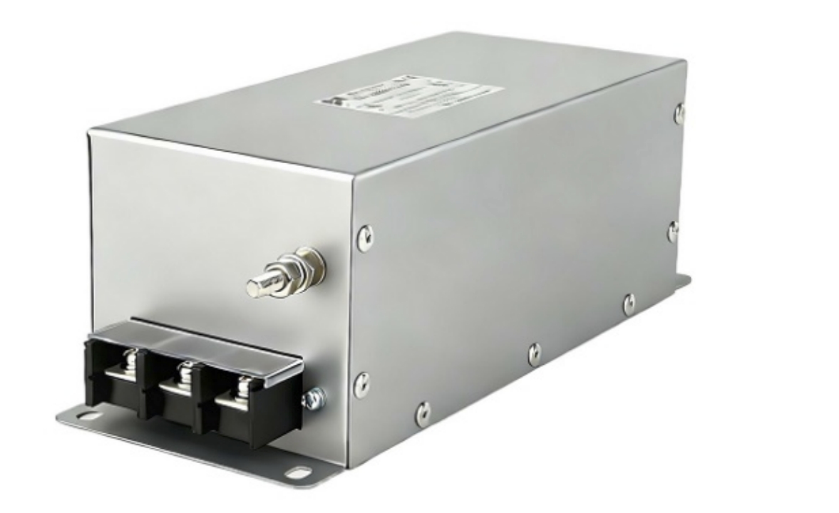
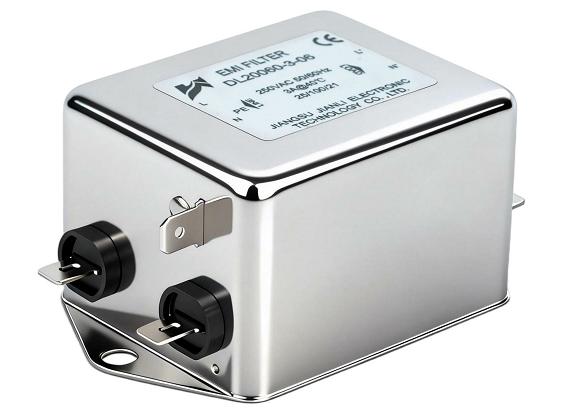
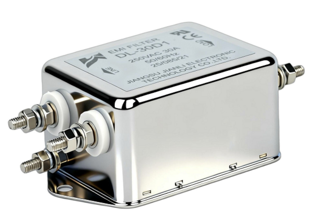
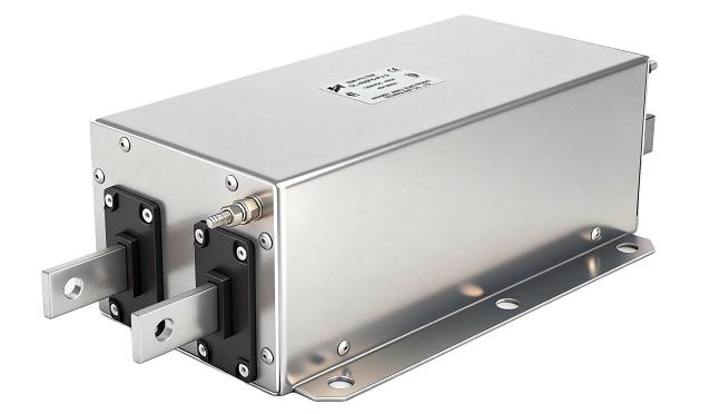
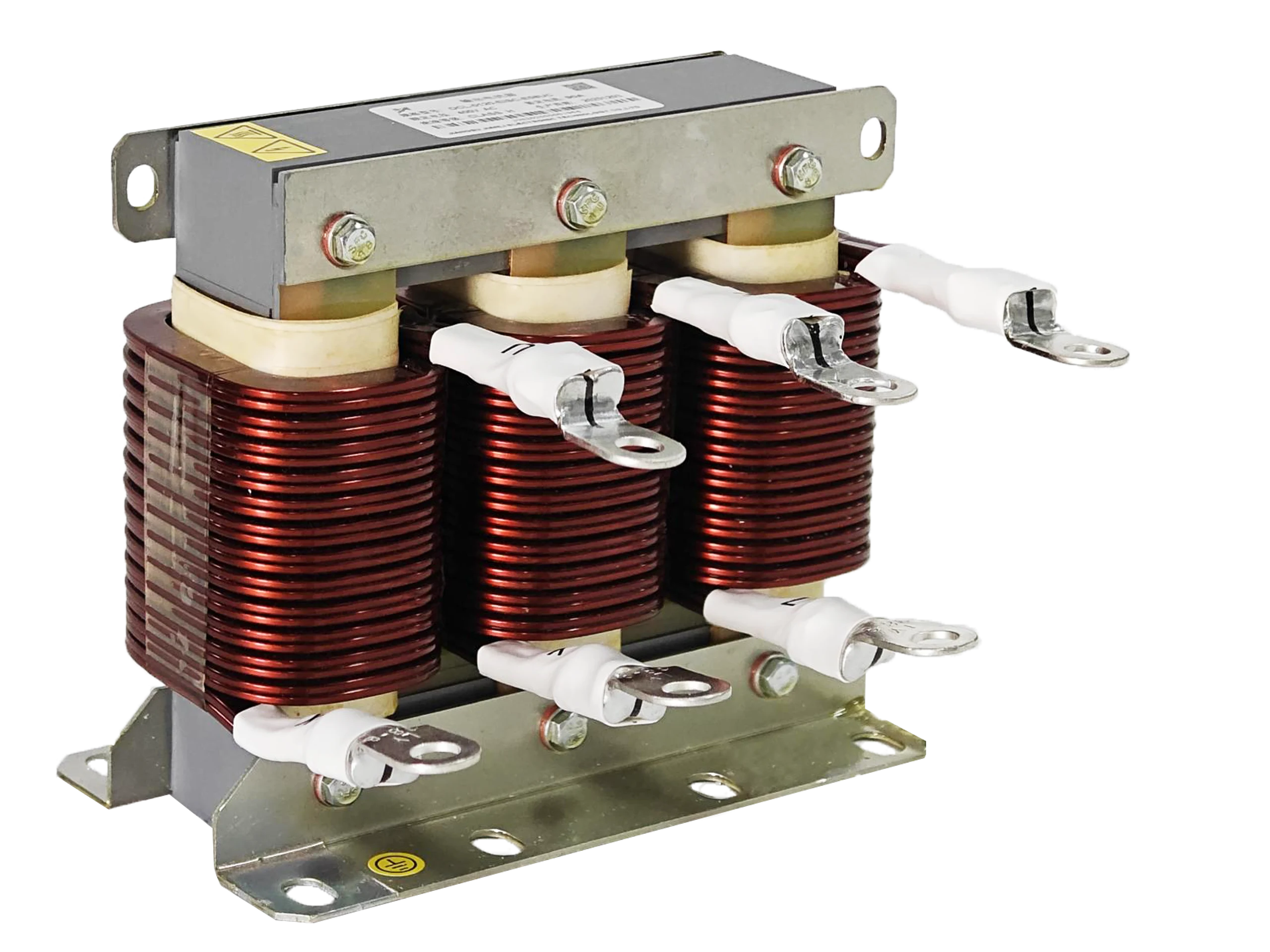
A PCB filter suppresses conducted and radiated EMI by attenuating unwanted high-frequency noise on signal and power lines. Correct component selection, topology, and placement determine whether a design passes CISPR 32, FCC Part 15, or IEC 61000 compliance testing.
What Is a PCB Filter and How Does It Work?
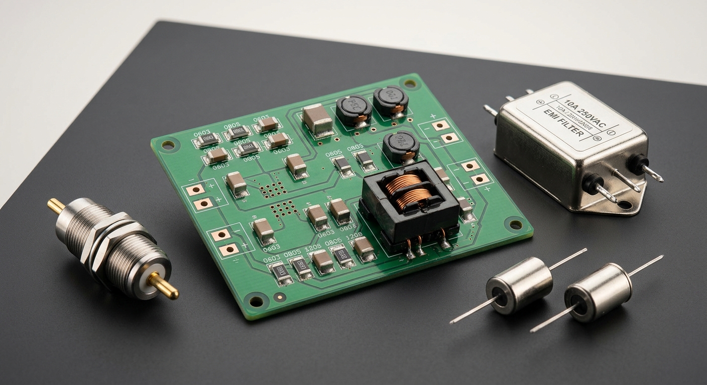
A PCB filter is a passive network—comprising capacitors, inductors, ferrite beads, or integrated LC arrays—mounted directly on a printed circuit board to attenuate electromagnetic interference before it propagates to other circuits or radiates from cable harnesses.
Core Attenuation Mechanisms
- Shunt capacitors divert high-frequency noise current to ground, effective from ~1 MHz upward.
- Series inductors present high impedance to noise current while passing DC and low-frequency signals.
- LC π-filters combine both mechanisms, achieving insertion loss >40 dB at target frequencies.
- Ferrite beads dissipate HF energy as heat; impedance peaks typically between 100 MHz–1 GHz.
Filter Topologies and Insertion Loss Comparison
| Topology | Typical Insertion Loss | Frequency Range | Best Use Case |
|---|---|---|---|
| Single capacitor (C) | 10–20 dB | 1–100 MHz | Low-cost, single-line filtering |
| L-filter (LC) | 20–35 dB | 500 kHz–500 MHz | Power entry, I/O lines |
| π-filter (CLC) | 40–60 dB | 1 MHz–1 GHz | Sensitive analog, RF circuits |
| T-filter (LCL) | 40–60 dB | 1 MHz–1 GHz | Low source/load impedance |
| Ferrite bead + cap | 25–45 dB | 10 MHz–3 GHz | Digital signal lines, USB, HDMI |
Differential vs. Common-Mode Noise
- Differential-mode (DM) noise flows between line and return; suppressed by series inductors and X-capacitors.
- Common-mode (CM) noise flows in the same direction on all conductors; suppressed by CM chokes and Y-capacitors.
- Most real-world EMI contains both modes; a well-designed PCB EMI suppression network addresses both simultaneously.
What Types of EMI Problems Can a PCB Filter Help Solve?
PCB filters address four primary interference categories encountered in electronic equipment design and EMC testing.
Conducted Emissions on Power Lines
Switching power supplies generate broadband noise from 150 kHz to 30 MHz. A PCB filter on the DC bus—typically a π-network with a CM choke—reduces conducted emissions to comply with CISPR 22/32 Class B limits (quasi-peak limit: 66 dBμV at 150 kHz, decreasing to 60 dBμV at 500 kHz).
High-Frequency Radiated Emissions
Clock harmonics above 30 MHz radiate from PCB traces acting as unintentional antennas. Ferrite beads (impedance 600 Ω at 100 MHz) on clock and data lines reduce trace current and lower radiated field strength by 6–15 dB.
Susceptibility and Immunity Failures
- ESD (IEC 61000-4-2): RC filters (100 Ω + 100 pF) on I/O lines limit transient energy entering sensitive ICs.
- EFT/Burst (IEC 61000-4-4): CM chokes with μH-range inductance attenuate 5/50 ns bursts on power and signal lines.
- Conducted immunity (IEC 61000-4-6): Low-pass filters on RF-exposed ports prevent in-band interference from coupling to internal circuits.
Signal Integrity Degradation
- Crosstalk and ground bounce in high-speed digital designs cause timing jitter and bit errors.
- Decoupling capacitors (100 nF ceramic, X7R) placed within 0.5 mm of IC power pins reduce power-plane impedance below 1 Ω up to 100 MHz.
PCB Filter Selection Guide for EMC Engineers
Selecting the correct PCB filter requires matching electrical parameters to the noise profile and circuit constraints.
Key Selection Parameters
| Parameter | Selection Criteria | Typical Range |
|---|---|---|
| Cutoff frequency (fc) | Below the lowest noise harmonic | 1 kHz – 100 MHz |
| Rated current | ≥125% of maximum load current | 0.1 A – 100 A |
| Rated voltage | ≥150% of operating voltage | 5 V – 1,000 V |
| Insertion loss @ target freq. | Must exceed emission margin | 20 – 60 dB |
| DCR (DC resistance) | Minimize voltage drop | 1 mΩ – 500 mΩ |
| Temperature rating | Exceeds ambient + self-heating | –40°C to +125°C |
How to Choose the Right PCB Filter Step by Step
- Measure the noise spectrum using a spectrum analyzer and LISN (Line Impedance Stabilization Network).
- Identify dominant mode (CM or DM) with a current probe; this determines choke vs. capacitor priority.
- Calculate required insertion loss: IL (dB) = measured emission level − regulatory limit + 6 dB safety margin.
- Select topology based on source/load impedance (high-Z source → C-input filter; low-Z source → L-input filter).
- Verify with SPICE simulation before prototype; model parasitic ESL and ESR of capacitors.
- Confirm thermal performance: Power dissipation in ferrite beads = I² × R(DC) + core losses at operating frequency.
Component-Level Considerations
- Ceramic capacitors (X7R/C0G): Stable capacitance vs. temperature; avoid Y5V in precision filters.
- Film capacitors: Lower ESR than ceramics for high-current applications; larger footprint.
- Integrated EMI filter arrays: Single-package LC networks save board space by up to 60% vs. discrete implementations.
Where to Place a PCB Filter for Maximum EMI Reduction
Placement is as critical as component selection. A correctly specified filter in the wrong location can be rendered ineffective by parasitic coupling.
Placement Rules
- At every board entry/exit point: Filters must be placed at the physical boundary where cables connect to the PCB—power connectors, I/O ports, RF interfaces.
- Guard-ring isolation: Surround filter components with a continuous ground pour connected to chassis ground via low-inductance vias (≤0.5 nH per via).
- Minimize trace length between filter and connector: Each 10 mm of unfiltered trace adds ~8 nH parasitic inductance, degrading HF performance.
- Separate clean and dirty ground planes: Use a single-point or split-plane topology to prevent re-contamination of filtered signals.
Layer Stack Considerations
| PCB Layer | Recommended Function | EMI Benefit |
|---|---|---|
| Layer 1 (top) | Signal routing, filter components | Short return paths |
| Layer 2 | Solid ground plane | Low-impedance reference |
| Layer 3 | Power plane | Distributed capacitance |
| Layer 4 (bottom) | Signal routing | Shielded by inner planes |
- A 4-layer stack with adjacent power-ground planes provides 20–30 dB additional HF noise suppression compared to a 2-layer board.
PCB Filter vs. Feedthrough Filter: Key Differences
Both devices suppress EMI, but they serve distinct roles in system-level EMC architecture.
Structural and Performance Comparison
| Attribute | PCB Filter | Feedthrough Filter |
|---|---|---|
| Mounting method | SMD or through-hole on PCB | Panel-mount, bulkhead, or inline |
| Ground connection | PCB ground plane | Metal chassis/enclosure |
| Insertion loss | 20–60 dB (topology-dependent) | 60–100 dB (direct chassis ground) |
| Frequency range | Up to 1–3 GHz | Up to 10 GHz |
| Current capacity | 0.1 A – 30 A typical | 1 A – 100+ A |
| Cost | Lower | Higher |
| Best application | Board-level filtering | System/enclosure boundary filtering |
- PCB filters are optimized for distributed, component-level noise suppression within a circuit.
- Feedthrough filters provide superior attenuation at enclosure penetration points because ground inductance is near zero (direct metal-to-metal bond).
- For TEMPEST or MIL-STD-461 compliance, feedthrough filters are mandatory at all enclosure penetrations.
Can a PCB Filter Help Electronic Products Pass EMC Testing?
Yes—when correctly designed and validated, PCB EMI suppression directly reduces both conducted and radiated emission levels and improves immunity test margins.
EMC Test Standards Addressed by PCB Filters
- CISPR 32 / EN 55032: Conducted emissions (150 kHz–30 MHz), radiated emissions (30 MHz–1 GHz).
- IEC 61000-3-2: Harmonic current limits; input filters reduce harmonic injection from SMPS.
- IEC 61000-4-2/4/5/6: ESD, EFT, surge, and conducted immunity; filters limit transient energy at I/O.
- FCC Part 15 Subpart B: Unintentional radiators; PCB filter selection guide for EMC engineers typically targets 6–10 dB margin above regulatory limits.
Practical EMC Test Improvement Data
- Adding a π-filter on a 12 V DC input reduced conducted emissions by 22 dB at 1 MHz in a motor controller application (measured per CISPR 25).
- Ferrite beads on USB 3.0 data lines reduced radiated emissions at the 2.5 GHz harmonic by 11 dB, enabling Class B compliance.
- CM choke (22 μH, 2 A) on AC input reduced Class B conducted emission exceedance from +14 dB to –3 dB margin.
FAQ: PCB Filter and EMI Suppression
What types of EMI problems can a PCB filter help solve?
Conducted emissions, radiated emissions, ESD susceptibility, and signal integrity degradation.
How do you choose the right PCB filter for an electronic circuit?
Match cutoff frequency, insertion loss, current rating, and topology to the measured noise spectrum.
Where should a PCB filter be placed to reduce EMI effectively?
At every board entry/exit point, adjacent to connectors, with minimal unfiltered trace length.
What is the difference between a PCB filter and a feedthrough filter?
PCB filters mount on the board; feedthrough filters bond directly to the chassis for higher attenuation.
Can a PCB filter help electronic products pass EMC testing?
Yes—properly selected filters reduce emissions by 10–40 dB, directly improving compliance margins.
What is the typical insertion loss of a PCB EMI filter?
20–60 dB depending on topology; π-filters achieve the highest attenuation.
Do ferrite beads count as PCB filters?
Yes—ferrite beads with bypass capacitors form a valid high-frequency PCB EMI suppression network.
What capacitor dielectric is best for PCB EMI filters?
C0G for precision low-loss; X7R for general-purpose decoupling up to 125°C.
Conclusion
A PCB filter is the most cost-effective, board-level tool for reducing electromagnetic interference in electronic equipment. Correct topology selection, component matching, and placement at board boundaries can reduce conducted emissions by 20–40 dB and improve radiated emission margins by 6–15 dB. Engineers should measure the noise spectrum first, calculate required insertion loss with a 6 dB safety margin, and validate with both simulation and pre-compliance testing before final EMC submission. For system-level isolation at enclosure boundaries, combine PCB filters with feedthrough filters to achieve the full attenuation required by CISPR 32, IEC 61000, and FCC Part 15 standards.
References and Standards
- CISPR 32:2015 — Electromagnetic compatibility of multimedia equipment
- IEC 61000-4-2:2008 — ESD immunity test
- IEC 61000-4-4:2012 — EFT/Burst immunity test
- IEC 61000-4-6:2013 — Conducted disturbances immunity
- FCC Part 15 Subpart B — Unintentional radiators
- MIL-STD-461G — EMC requirements for military equipment
- Ott, H.W. Electromagnetic Compatibility Engineering. Wiley, 2009.
- Williams, T. EMC for Product Designers, 5th ed. Newnes, 2017.